- 您现在的位置:买卖IC网 > Sheet目录3841 > PIC16F737-I/SP (Microchip Technology)IC PIC MCU FLASH 4KX14 28DIP
2004 Microchip Technology Inc.
DS30498C-page 21
PIC16F7X7
2.2.2.1
Status Register
The Status register contains the arithmetic status of the
ALU, the Reset status and the bank select bits for data
memory.
The Status register can be the destination for any
instruction, as with any other register. If the Status
register is the destination for an instruction that affects
the Z, DC or C bits, then the write to these three bits is
disabled. These bits are set or cleared according to the
device logic. Furthermore, the TO and PD bits are not
writable, therefore, the result of an instruction with the
Status register as destination may be different than
intended.
For example, CLRF STATUS, will clear the upper three
bits and set the Z bit. This leaves the Status register as
000u u1uu
(where u = unchanged).
It is recommended, therefore, that only BCF, BSF,
SWAPF
and MOVWF instructions are used to alter the
Status register because these instructions do not affect
the Z, C or DC bits from the Status register. For other
instructions
not
affecting
any
Status
bits,
see
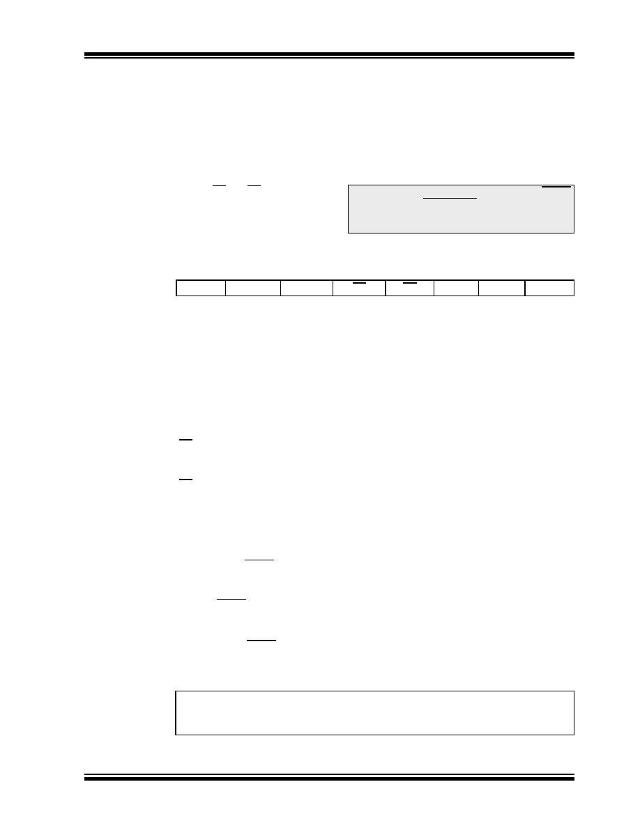
REGISTER 2-1:
STATUS: ARITHMETIC STATUS REGISTER (ADDRESS 03h, 83h, 103h, 183h)
Note 1: The C and DC bits operate as a borrow
and digit borrow bit, respectively, in
subtraction. See the SUBLW and SUBWF
instructions for examples.
R/W-0
R-1
R/W-x
IRP
RP1
RP0
TO
PD
ZDC
C
bit 7
bit 0
bit 7
IRP: Register Bank Select bit (used for indirect addressing)
1
= Bank 2, 3 (100h-1FFh)
0
= Bank 0, 1 (00h-FFh)
bit 6-5
RP1:RP0: Register Bank Select bits (used for direct addressing)
11
= Bank 3 (180h-1FFh)
10
= Bank 2 (100h-17Fh)
01
= Bank 1 (80h-FFh)
00
= Bank 0 (00h-7Fh)
Each bank is 128 bytes.
bit 4
TO: Time-out bit
1
= After power-up, CLRWDT instruction or SLEEP instruction
0
= A WDT time-out occurred
bit 3
PD: Power-Down bit
1
= After power-up or by the CLRWDT instruction
0
= By execution of the SLEEP instruction
bit 2
Z: Zero bit
1
= The result of an arithmetic or logic operation is zero
0
= The result of an arithmetic or logic operation is not zero
bit 1
DC: Digit Carry/borrow bit (ADDWF, ADDLW, SUBLW, SUBWF instructions)
1
= A carry-out from the 4th low-order bit of the result occurred
0
= No carry-out from the 4th low-order bit of the result
bit 0
C: Carry/borrow bit (ADDWF, ADDLW, SUBLW, SUBWF instructions)
1
= A carry-out from the Most Significant bit of the result occurred
0
= No carry-out from the Most Significant bit of the result occurred
Note:
For borrow, the polarity is reversed. A subtraction is executed by adding the
two’s complement of the second operand. For rotate (RRF, RLF) instructions, this
bit is loaded with either the high or low-order bit of the source register.
Legend:
R = Readable bit
W = Writable bit
U = Unimplemented bit, read as ‘0’
-n = Value at POR
‘1’ = Bit is set
‘0’ = Bit is cleared
x = Bit is unknown
发布紧急采购,3分钟左右您将得到回复。
相关PDF资料
PIC18F86K22-I/PTRSL
MCU PIC 64K FLASH XLP 80TQFP
PIC16C63A-04I/SP
IC MCU OTP 4KX14 PWM 28DIP
PIC16C63A-04I/SO
IC MCU OTP 4KX14 PWM 28SOIC
52559-2270
CONN FFC 22POS .5MM VERT ZIF SMD
52559-1870
CONN FFC 18POS .5MM VERT ZIF SMD
DSPIC33EP64MC506-I/PT
IC DSC 16BIT 64KB FLASH 64TQFP
52745-1896
CONN FFC 18POS .5MM R/A ZIF SMD
PIC16LC622-04/P
IC MCU OTP 2KX14 COMP 18DIP
相关代理商/技术参数
PIC16F737-I/SP
制造商:Microchip Technology Inc 功能描述:IC 8BIT FLASH MCU 16F737 SDIL28
PIC16F737-I/SS
功能描述:8位微控制器 -MCU 7KB 368 RAM 25 I/O RoHS:否 制造商:Silicon Labs 核心:8051 处理器系列:C8051F39x 数据总线宽度:8 bit 最大时钟频率:50 MHz 程序存储器大小:16 KB 数据 RAM 大小:1 KB 片上 ADC:Yes 工作电源电压:1.8 V to 3.6 V 工作温度范围:- 40 C to + 105 C 封装 / 箱体:QFN-20 安装风格:SMD/SMT
PIC16F737T-I/ML
功能描述:8位微控制器 -MCU 7KB 368 RAM 25 I/O RoHS:否 制造商:Silicon Labs 核心:8051 处理器系列:C8051F39x 数据总线宽度:8 bit 最大时钟频率:50 MHz 程序存储器大小:16 KB 数据 RAM 大小:1 KB 片上 ADC:Yes 工作电源电压:1.8 V to 3.6 V 工作温度范围:- 40 C to + 105 C 封装 / 箱体:QFN-20 安装风格:SMD/SMT
PIC16F737T-I/SO
功能描述:8位微控制器 -MCU 7KB 368 RAM 25 I/O RoHS:否 制造商:Silicon Labs 核心:8051 处理器系列:C8051F39x 数据总线宽度:8 bit 最大时钟频率:50 MHz 程序存储器大小:16 KB 数据 RAM 大小:1 KB 片上 ADC:Yes 工作电源电压:1.8 V to 3.6 V 工作温度范围:- 40 C to + 105 C 封装 / 箱体:QFN-20 安装风格:SMD/SMT
PIC16F737T-I/SS
功能描述:8位微控制器 -MCU 7KB 368 RAM 25 I/O RoHS:否 制造商:Silicon Labs 核心:8051 处理器系列:C8051F39x 数据总线宽度:8 bit 最大时钟频率:50 MHz 程序存储器大小:16 KB 数据 RAM 大小:1 KB 片上 ADC:Yes 工作电源电压:1.8 V to 3.6 V 工作温度范围:- 40 C to + 105 C 封装 / 箱体:QFN-20 安装风格:SMD/SMT
PIC16F73-E/ML
功能描述:8位微控制器 -MCU 7 KB 368 RAM 25I/O RoHS:否 制造商:Silicon Labs 核心:8051 处理器系列:C8051F39x 数据总线宽度:8 bit 最大时钟频率:50 MHz 程序存储器大小:16 KB 数据 RAM 大小:1 KB 片上 ADC:Yes 工作电源电压:1.8 V to 3.6 V 工作温度范围:- 40 C to + 105 C 封装 / 箱体:QFN-20 安装风格:SMD/SMT
PIC16F73-E/SO
功能描述:8位微控制器 -MCU 7KB 192 RAM 22 I/O RoHS:否 制造商:Silicon Labs 核心:8051 处理器系列:C8051F39x 数据总线宽度:8 bit 最大时钟频率:50 MHz 程序存储器大小:16 KB 数据 RAM 大小:1 KB 片上 ADC:Yes 工作电源电压:1.8 V to 3.6 V 工作温度范围:- 40 C to + 105 C 封装 / 箱体:QFN-20 安装风格:SMD/SMT
PIC16F73-E/SP
功能描述:8位微控制器 -MCU 7KB 192 RAM 22 I/O RoHS:否 制造商:Silicon Labs 核心:8051 处理器系列:C8051F39x 数据总线宽度:8 bit 最大时钟频率:50 MHz 程序存储器大小:16 KB 数据 RAM 大小:1 KB 片上 ADC:Yes 工作电源电压:1.8 V to 3.6 V 工作温度范围:- 40 C to + 105 C 封装 / 箱体:QFN-20 安装风格:SMD/SMT